Complementary short courses at Nordpac 2023
At NordPac 2023 we have the pleasure of offering two short courses. These will be free of charge for all participants that have registered for the full conference.
Both courses will be held on Monday the 12th of June at Oslo Science Park. A complimentary lunch will be served.
| Time | Course title | About the author |
| 09:00 – 12:00 |
Fan-out, Fan-in, and Heterogeneous Integration Packaging
|
 John H Lau, with more than 40 years of R&D and manufacturing experience in semiconductor packaging and SMT assembly, has published more than 515 peer-reviewed papers (375 are the principal investigator), 40 issued and pending US patents (25 are the principal inventor), and 23 textbooks (all are the first author) on, e.g., Advanced MEMS Packaging (McGraw-Hill, 2010), Reliability of RoHS compliant 2D & 3D IC Interconnects (McGraw-Hill, 2011), Through-Silicon Via (TSV) for 3D Integration (McGraw-Hill, 2013), 3D IC Integration and Packaging (McGraw-Hill, 2016), and Assembly and Reliability of Lead-Free Solder Joints (Springer, 2020). John is an elected IEEE fellow, IMAPS Fellow, and ASME Fellow and has been actively participating in industry/academy/society meetings/conferences to contribute, learn, and share. John H Lau, with more than 40 years of R&D and manufacturing experience in semiconductor packaging and SMT assembly, has published more than 515 peer-reviewed papers (375 are the principal investigator), 40 issued and pending US patents (25 are the principal inventor), and 23 textbooks (all are the first author) on, e.g., Advanced MEMS Packaging (McGraw-Hill, 2010), Reliability of RoHS compliant 2D & 3D IC Interconnects (McGraw-Hill, 2011), Through-Silicon Via (TSV) for 3D Integration (McGraw-Hill, 2013), 3D IC Integration and Packaging (McGraw-Hill, 2016), and Assembly and Reliability of Lead-Free Solder Joints (Springer, 2020). John is an elected IEEE fellow, IMAPS Fellow, and ASME Fellow and has been actively participating in industry/academy/society meetings/conferences to contribute, learn, and share. |
|
Fan-out wafer/panel-level packaging has been getting lots of tractions since TSMC used their integrated fan-out to package the application processor chipset for the iPhone 7. In this lecture, the following topics will be presented and discussed. Emphasis is placed on the fundamentals and latest developments of these areas in the past few years. Fan-in packaging has been used for many years. Their future trends will also be explored. In this lecture, a six-side molded fan-in wafer level package and its reliability will be presented. Heterogeneous integration (HI) uses packaging technology to integrate dissimilar chips, photonic devices, and/or components (either side-by-side, stacked, or both) with different sizes and functions, and from different fabless design houses, foundries, wafer sizes, and feature sizes into a system or subsystem on a common package substrate. For the next few years, we will see more implementations of a higher level of HI packaging, whether it is for time-to-market, performance, form factor, power consumption or cost. In this lecture, the introduction, recent advances, and trends in HI packaging will be presented. Course Outline:
Who Should Attend? If you (students, engineers, and managers) are involved with any aspect of the electronics industry, you should attend this course. It is equally suited for R&D professionals and scientists. The lectures are based on the publications by many distinguish authors and the books (by the lecturer) such as Fan-Out Wafer-Level Packaging (Springer, 2018), Heterogeneous Integration (Springer, 2019), Semiconductor Advanced Packaging (Springer, 2021). and Chiplet Design and Heterogeneous Integration Packaging (Springer, 2023). Each attendee will receive more than 200 pages of lecture notes. |
||
| 12:00 – 13:00 | Lunch | |
| 13:00 – 16:00 |
Solid-Liquid Interdiffusion (SLID) Bonding – for Challenges in Microsystem Bonding
|
Knut Eilif Aasmundtveit (University of SouthEast Norway) & Vesa Vuorinen (Aalto University).
During the last decade, his research has been focusing on materials compatibility in heterogeneous systems with the emphasis on interfacial phenomena. He has also been responsible for teaching physics of failure and reliability assessment in electronics and direct research cooperation with the industrial partners for the last twenty years. He has been involved in the creation of international electronics assembly technology standards (IEC) and contributed to two text books dealing with interfacial compatibility issues and thermodynamics of solid state diffusion as well as authored or co-authored over 60 scientific papers and several book chapters. He is also a co-founder of a company called Compatian, which offers consulting services for industry in the field of demanding reliability and materials scientific problems.
|
| Solid-Liquid InterDiffusion (SLID) bonding for microelectronics and microsystems is a bonding technique relying on binary (or ternary) metal systems reacting to intermetallics. The high melting temperature of intermetallics allows for system operation at far higher temperatures than what solder-bonded systems can do, while still using similar process temperatures as in common solder processes. Additional benefits of SLID bonding are possibilities of fine-pitch bonding, as well as thin-layer metallurgical bonding.
The short course aims at sharing the experience obtained at USN and Aalto after more than a decade of research. The material systems include Cu–Sn, Au–Sn, and low-temperature SLID systems with In, In–Sn or In–Bi as the low-temperature metal. Examples of system-level implementation of SLID bonding includes wafer-level vacuum sealing of MEMS bolometers, as well as lamination of ultrasound transducers. Fundamental work to be shared during the short course includes phase determination of SLID bonds, with emphasis on Au–Sn, reliability verification, as well as experimental verification of high-temperature stability for a number of SLID systems. Moreover, the process integration challenges, the formation of residual stresses and low-temperature SLID options will also be addressed. |
||
Registration
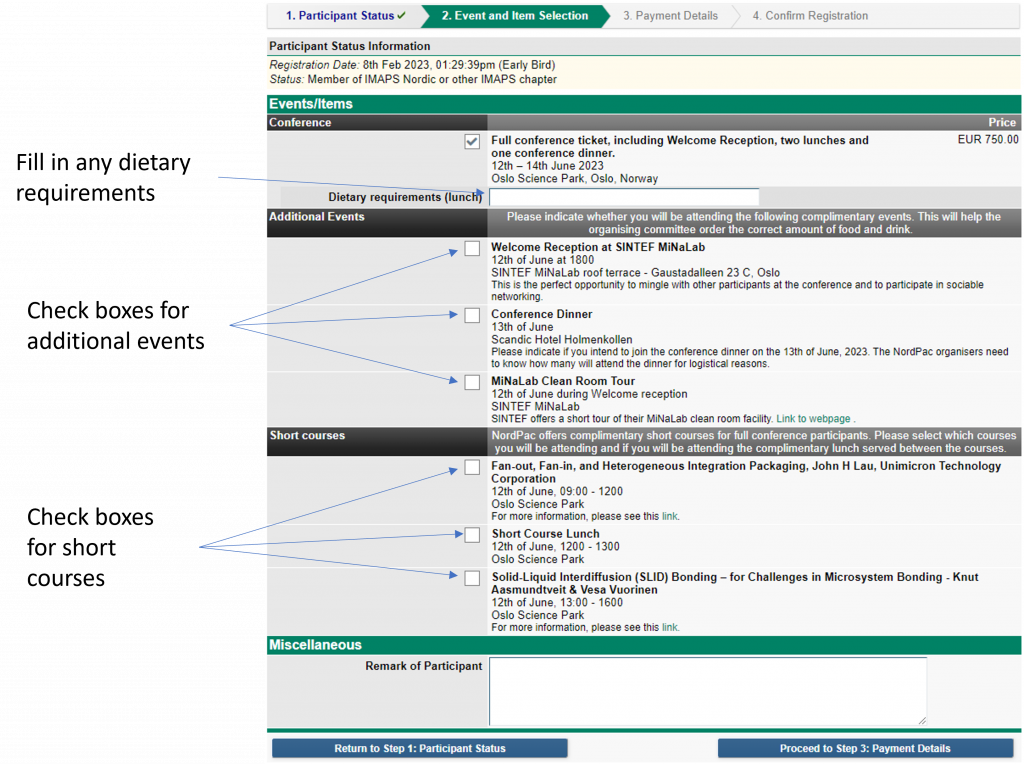
To register for the short courses, simply select these events during the registration to the conference. Your selection can be edited at a later time, so if you are hindered from coming due to change of plans, please edit your entry accordingly. Remember to add any dietary requirements if needed.


 Knut E. Aasmundtveit received the M.Sc. degree in technical physics from the Norwegian Institute of Technology, Trondheim, Norway, in 1994, and the Ph.D. degree in materials physics from the Norwegian University of Science and Technology, Trondheim, in 1999. He was with Kongsberg Norspace, Horten, Norway, as RF System Design Engineer until 2004. He then joined the University of South-Eastern Norway (then: Vestfold University College) as Associate Professor, becoming Professor in 2013. He has authored or coauthored six book chapters and more than 100 journal and conference papers. His research interests include packaging and integration technology for micro- and nanosystems, such as intermetallic bonding, polymer-based bonding, nanomaterials integration in microsystems, as well as biomedical packaging. General Chair of ESTC 2020 (IEEE EPS), he presently serves as member of the ESTC Steering Committee.
 Dr. Vesa Vuorinen (born 1971, Finland) received his M.Sc. degree 1995 in Materials Science and Engineering and D.Sc. (Tech.) degree in 2006 in the Department of Electronics from the former Helsinki University of Technology. Currently he is working in Aalto University as senior university lecturer and project manager in the research group of Electronics Integration and Reliability.
